Feb 17, 2023 Update
Executive Summary
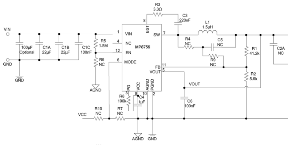
Details
To make sure we didn't have problems below is are some rough design calculations per the sometimes correct datasheet.
import Text.Printf

-- We don't want to blow up the chip
-- so compute vEN to be sure that
--     4.0 > vEN > 1.4
vIn = 12
r6 = 300e3
pullDown = 600e3
rp = (r6 * pullDown) / (r6 + pullDown)
vEN = (vIn * rp) / (1.5e6 + 600)
printf "vEN at 12V -> %5.2f" vEN
printf "vEN at 24V -> %5.2f" (2*vEN)
vEN at 12V -> 1.60
vEN at 24V -> 3.20
r6 at 300k yields a good vEN for 12 and 24v
vRef = 600e-3
r1 = 41.2e3

-- Calculate R2 for output volage of 5V
r2 = (vRef * r1) / (5.0 - 0.6)
printf "r2 = %5.2f" r2
r2 = 5618.18
Board values for FB resistors are correct for Vout is 5v.
vPG = 0.4 -- at I = 4ma
vCC = 3.6 -- nominal
Inductor Choice
fSW = 700e3
deltaI = 2.8 -- 30% of output current
vOut = 5.0
vIn = 12.0
indL = (vOut/(fSW*deltaI)) * (1.0-(vOut/vIn))
printf "L -> %5.2e" indL
L -> 1.49e-6
This means that the ripple current will be 2.8 amps
Peak Inductor Current
iOut = 6.0
iPeak = iOut + (vOut / (2.0 * fSW * indL)) * (1.0 - (vOut / vIn))
printf "Ipeak -> %5.2e" iPeak
putStrLn "This is below the max switch current of 10A"
Ipeak -> 7.40e0
This is below the max switch current of 10A
Power Good Circuit
The VCC output is 3.6 volts and the $V_f$ of the LED is 1.8V so the series resistor should be approximatly,
rLED = (3.6 - 1.8 - 0.4) / 4e-3
printf "LED series resistor -> %5.2f" rLED
putStrLn "So make it 330 for about 4ma"
LED series resistor -> 350.00
So make it 330 for about 4ma
Talked with Joey.